I went to a university career advisor at some point wanting help breaking into the semiconductor industry. The advice I got was to practice LeetCode and apply for software engineering roles.
That was the moment I realized there was no pathway at all. If you wanted to go into silicon fabrication, physical design, electronic design automation (EDA), or process integration, you were completely on your own. University career services treated all “tech” as interchangeable web development, leaving hardware engineering students to navigate an opaque, capital-intensive industry without an institutional roadmap.
Getting it off the groundI wasn’t sure the demand was there at the scale needed to make it real. The career centre’s response had suggested the institution didn’t think so either. What I had was a series of direct conversations with students who wanted exactly what I was describing, and I treated that as enough. It was.
1. The Broken Paradigm: Why Software Advice Fails Hardware Engineers
The structural divide between software engineering and semiconductor engineering is absolute. In software, an entry-level candidate can spin up an AWS instance, write a full-stack application, and grind dynamic programming problems on LeetCode to clear technical screens.
In semiconductors, that paradigm is useless:
========================================================================================
THE THREE PILLARS OF THE SEMICONDUCTOR ECOSYSTEM
========================================================================================
1. FABRICATION & PROCESS (Foundries: TSMC, GlobalFoundries, UMC)
   • Lithography (EUV/DUV), Plasma Etch, Chemical Vapor Deposition (CVD), CMP
   • Defect density, metrology, statistical process control (SPC), yield optimization
   • Metric: Wafers per hour, defect count/cm², parametric yield

2. IC DESIGN & VERIFICATION (Fabless: AMD, Nvidia, Qualcomm, Apple)
   • Frontend: RTL design (Verilog / SystemVerilog), UVM verification testbenches
   • Backend: Logic synthesis, Static Timing Analysis (STA), Clock Tree Synthesis (CTS)
   • Metric: WNS / TNS (Timing Slack), dynamic power (mW), cell density / mm²

3. ELECTRONIC DESIGN AUTOMATION (Tooling: Synopsys, Cadence, Siemens EDA)
   • Computational geometry, SAT solvers, graph-theoretic place-and-route engines
   • Transistor-level SPICE simulation, parasitic extraction (RC extraction)
   • Metric: Tool convergence runtime, simulation throughput, GDSII precision
========================================================================================
No semiconductor team interviews candidates on reversing a linked list. They care whether an engineer can debug hold violations across clock domains, interpret a static timing report, reason about CMOS latch-up, or understand how plasma etch selectivity impacts wafer yield.
Singapore accounts for approximately 11% of the world’s global semiconductor market and 20% of global semiconductor manufacturing equipment. Yet, despite NTU training hundreds of electrical engineers annually, students either drifted into generic software roles or struggled to identify the difference between an analog layout engineer and a field application engineer. We founded the NTU Semiconductor Club to bridge this knowledge chasm.
2. Institutional Navigation: Constitution & Faculty Sponsorship
Establishing a new engineering society within NTU required navigating university governance across the Student Affairs Office (SAO) and the School of Electrical and Electronic Engineering (EEE).
Drafting the Constitution
A club cannot survive on student enthusiasm alone; it requires operational structure. I drafted the founding constitution from scratch, defining:
- Technical Divisions: Establishing distinct tracks for Digital VLSI & Architecture, Process & Fabrication, and Industry Partnerships.
- Governance & Succession: Transparent election bylaws, executive committee accountability, and peer-to-peer technical workshop requirements to ensure continuity past our graduation.
- Ethics & Lab Hygiene: Strict safety protocols governing student conduct during cleanroom visits and industrial lab sessions.
Faculty Negotiations
Convincing tenured professors to formally sponsor a new organization requires speaking the institution’s language. University administrations do not grant charters for vague hobby clubs; they respond to measurable institutional outcomes:
- Graduate Placement Rates: Demonstrating how dedicated industry pipelines directly improve high-value engineering employment in multinational semiconductor firms.
- Curriculum Augmentation: Framing the club as a practical testbed that bridges theoretical textbook physics with hands-on EDA and cleanroom experience.
- Industry Alignment: Tying our charter directly to Singapore’s national focus on semiconductor workforce development.
After multiple rounds of pitches, we secured our faculty advisor, gained formal institutional chartering, and unlocked departmental room bookings and seed funding.
3. Demystifying the Fab: Cleanroom Clearance at N2FC
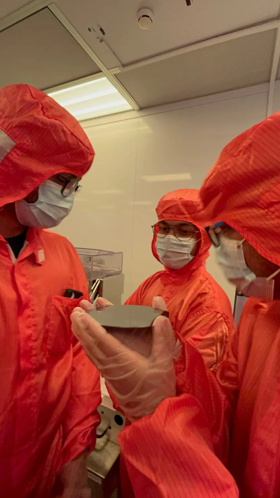
Theoretical device physics in a lecture hall cannot substitute for standing inside a cleanroom. One of our highest operational priorities was securing undergraduate access to the NTU Nanofabrication Centre (N2FC), a Class 100 / Class 1000 research facility equipped with advanced photolithography, thin-film deposition, and characterization equipment.
Overcoming Safety & Chemical Barriers
Cleanroom access is heavily restricted due to severe chemical hazards, including hydrofluoric acid (HF), piranha solution, and toxic precursor gases (silane, phosphine).
To make student visits feasible:
- Worked with N2FC safety officers to design a standardized cleanroom protocol briefing covering hazardous chemical exposure, emergency eyewash/shower procedures, and evacuation paths.
- Enforced strict cleanroom gowning discipline (bunny suits, antistatic hoods, booties, nitrile gloves) to prevent particulate contamination ($<100$ particles ≥ 0.5\mum per cubic foot) on active wafer chucks.
- Led cohorts of 40+ members through live demonstrations of spin-coaters, mask aligners, plasma-enhanced chemical vapor deposition (PECVD) reactors, and scanning electron microscopy (SEM) inspection stations.
For most members, this was their first time seeing a raw silicon wafer and experiencing the physical reality of semiconductor manufacturing.
4. Engineering Technical Industry Pipelines
We bypassed generic career fairs and built direct technical engagements with semiconductor leaders, ensuring every event delivered deep technical insight rather than generic HR slides.
AMD: Advanced Packaging & Silicon Validation
We organized technical immersions with AMD Singapore, focusing on modern heterogeneous compute architectures.
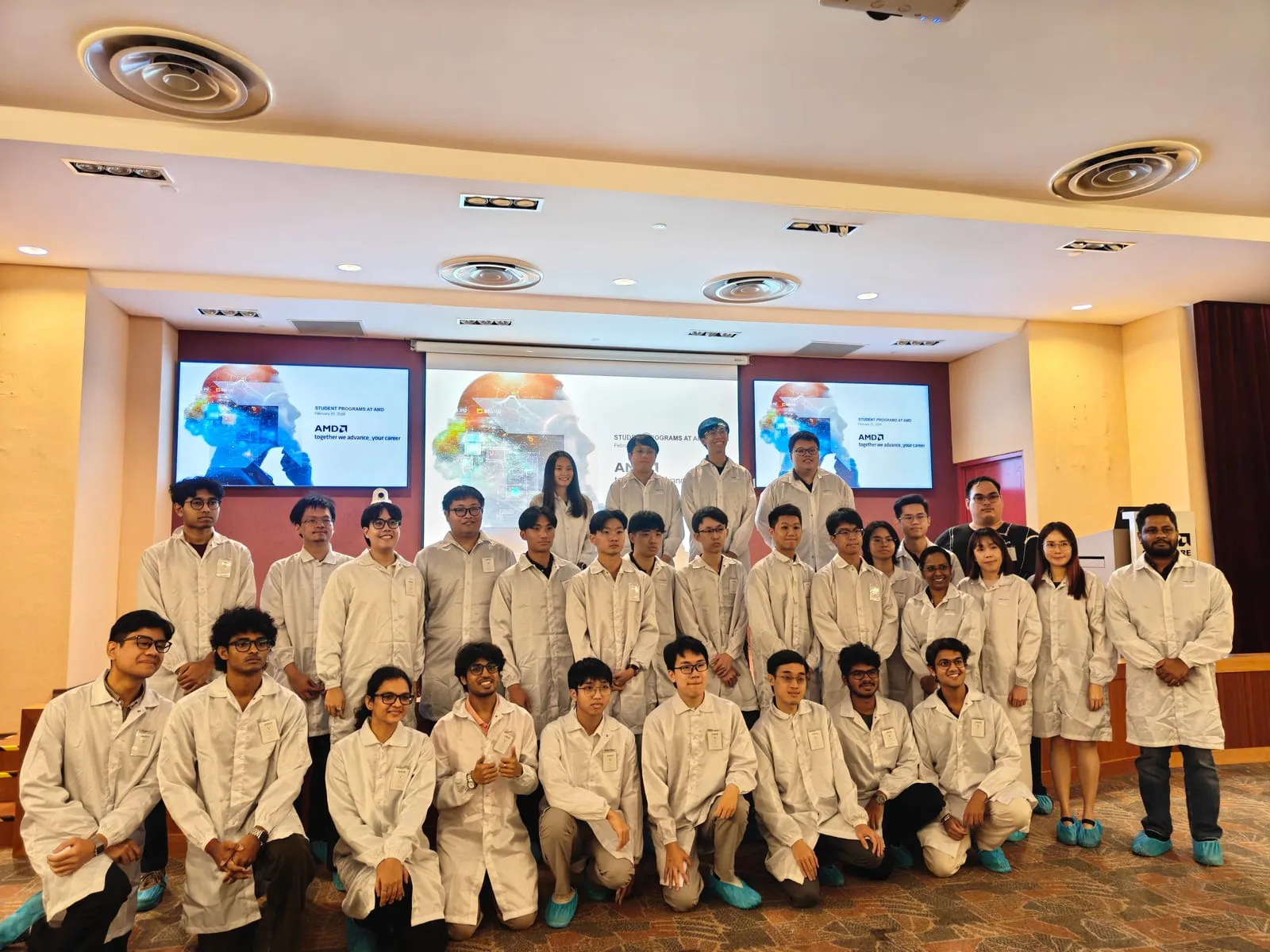
Engineers walked our members through:
- 2.5D/3D Chiplet Stacking: Moving beyond monolithic dies to high-density silicon interposers bridging CPU compute cores with High-Bandwidth Memory (HBM).
- Post-Silicon Validation: How automated test equipment (ATE) and scan chains (Boundary Scan / JTAG) identify manufacturing defects before chips are packaged and shipped.
GlobalFoundries: 300mm Fab Floor Immersion
We brought club cohorts directly onto the manufacturing floor at GlobalFoundries’ 300mm wafer fabrication facility in Singapore.
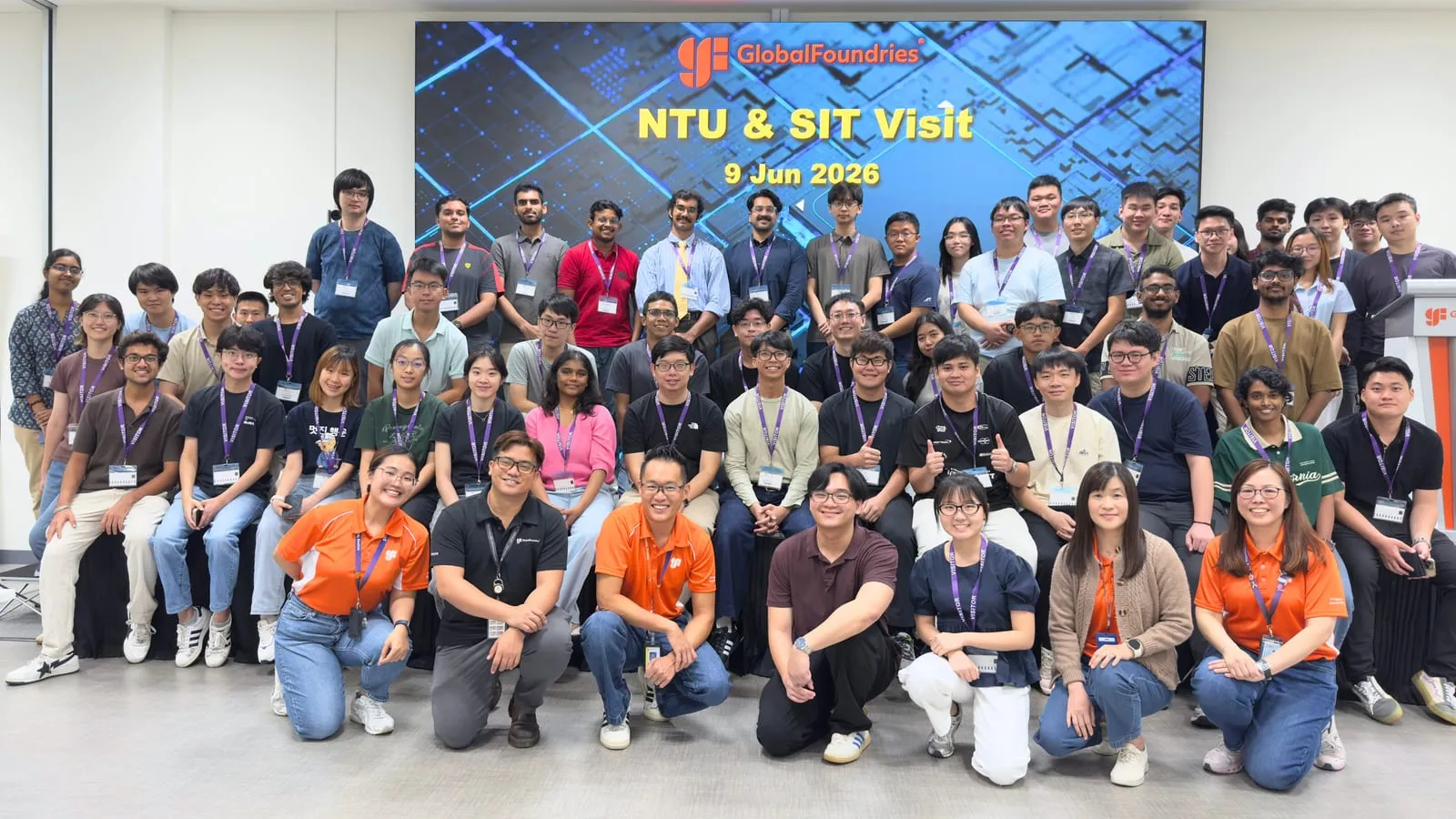
Members observed:
- Automated Material Handling Systems (AMHS): Overhead robotic tracks transporting Front Opening Unified Pods (FOUPs) filled with 300mm wafers between lithography, etch, and diffusion bays.
- Statistical Process Control (SPC): How real-time yield telemetry monitors particulate counts, critical dimensions (CD), and chemical bath temperatures to prevent wafer scrap.
AI Singapore (AISG): Silicon for Deep Learning
Recognizing that modern AI models are constrained by hardware memory bandwidth, we partnered with AI Singapore for cross-disciplinary technical seminars.
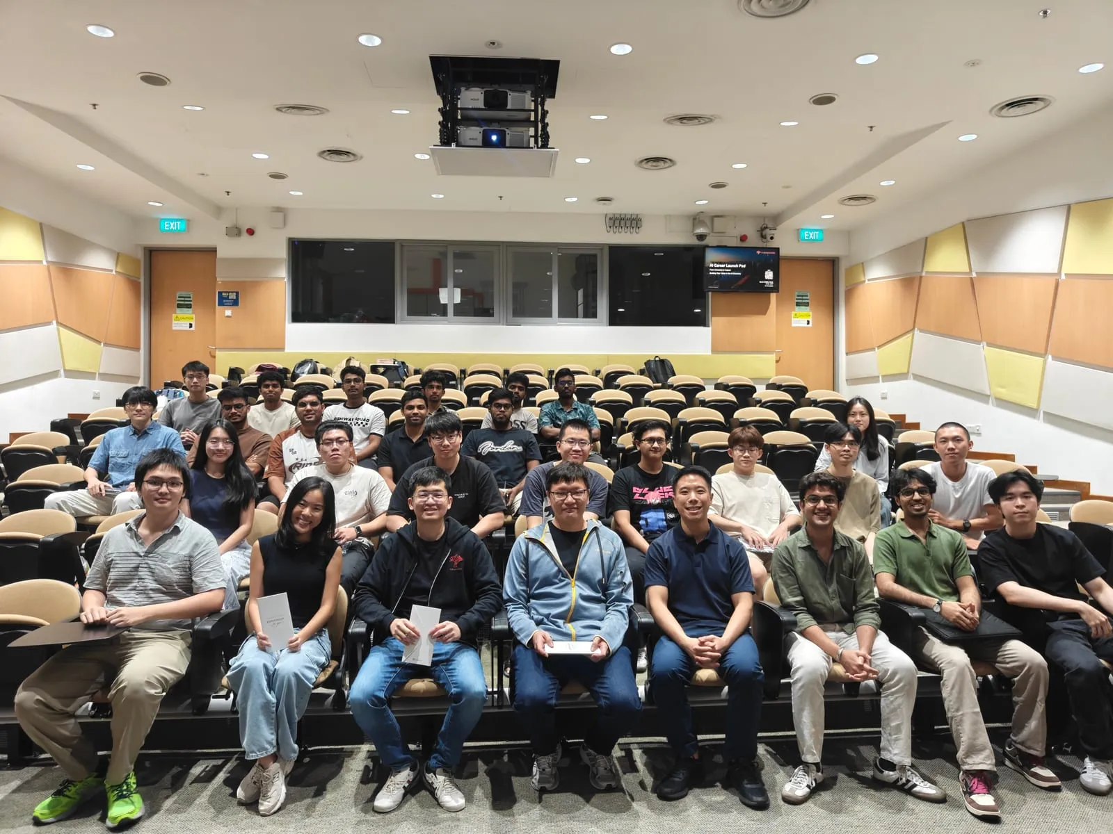
The sessions explored how transformer models demand specialized hardware accelerators (systolic arrays, quantized integer ALUs, and massive memory bandwidth), connecting software AI practitioners with underlying chip design realities.
5. Scaling to 400 Members & Hands-On Technical Workshops
To sustain engagement between company visits, we launched peer-led technical bootcamps. Rather than relying on costly proprietary EDA licenses that lock students out of experimenting on personal machines, we developed a curriculum around open-source tooling:
┌────────────────────────────────────────────────────────────────────────────────────────┐
│ NTU SEMICONDUCTOR CLUB TECHNICAL CURRICULUM                                            │
│                                                                                        │
│   ┌───────────────────────────┐   ┌──────────────────────┐   ┌─────────────────────┐   │
│   │ Track 1: Digital RTL      │   │ Track 2: Open EDA    │   │ Track 3: Process    │   │
│   │ • Verilog-2001 & SV       │   │ • Yosys Synthesis    │   │ • Cleanroom safety  │   │
│   │ • Pipelined CPU design    │──►│ • OpenROAD P&R Flow  │──►│ • Litho / Etch flow │   │
│   │ • Vivado FPGA synthesis   │   │ • SkyWater 130nm PDK │   │ • N2FC lab sessions │   │
│   └───────────────────────────┘   └──────────────────────┘   └─────────────────────┘   │
└────────────────────────────────────────────────────────────────────────────────────────┘- Verilog & FPGA Labs: Stepping members through building finite state machines, memory controllers, and pipelined RISC architectures on Artix-7 FPGAs.
- Open-Source RTL-to-GDSII: Teaching synthesis and place-and-route using Yosys, OpenROAD, and the SkyWater 130nm open PDK, allowing students to generate tapeout-ready GDSII layouts on their personal laptops.
- Domain-Specific Networking: Segmenting sessions into specialized roundtables (analog IC, digital frontend, physical design, and fab engineering) so members could target specific industry subfields.
Where it standsFrom a blank page and a rejected career advice meeting to 400 active members, sustained semesterly industry pipelines, cleanroom access, and regular technical workshops. The semiconductor pathway at NTU now exists.
Club Operations & Technical Stack
- Student Body: 400+ active members across EEE, CCDS, MSE, and Physics departments
- Industry Partners: AMD, GlobalFoundries, AI Singapore, Micron, MediaTek
- Laboratory Facilities: NTU Nanofabrication Centre (N2FC) Class 100/1000 Cleanrooms
- Workshop Tooling: Verilog-2001, SystemVerilog, Xilinx Vivado, Yosys, OpenROAD, SkyWater 130nm PDK